

UV Cleaning and UV Exposure in Semiconductor and Electronics Manufacturing
Ultraviolet radiation serves two fundamentally different purposes in semiconductor and electronics manufacturing: the dry, photochemical cleaning and activation of surfaces, and the exposure of radiation-sensitive layers. In semiconductor UV cleaning, organic adsorbates are oxidatively decomposed to CO₂ and H₂O by short-wavelength photons and the reactive oxygen species they generate, without any mechanical or wet-chemical stress. In the UV exposure of photoresist, the absorbed photon dose governs the chemical conversion of the photoactive compound and thus edge profile and critical dimension.
Both processes are determined by the same quantities: spectral irradiance at the point of process, radiant exposure, the absorption behaviour of the material, the geometry of the irradiation gap and the composition of the process atmosphere. The central challenge is that none of these quantities can be reliably derived from electrical lamp power or process time.

How is the market for semiconductor manufacturing and UV process technology developing?
There is no standalone, cleanly delimited market statistic for UV cleaning, wafer activation and photoresist exposure. What is reliable instead are market indicators from the adjacent capital equipment markets, which determine the number and demand density of the process steps concerned.
| Market indicator | Value | Time reference | Source (year) |
|---|---|---|---|
| Global semiconductor market | around USD 1.5 trillion, driven by memory and AI infrastructure | forecast 2026 | WSTS, Spring Forecast (2026) |
| Semiconductor manufacturing equipment, total | USD 165.9 billion, +23.2 % | forecast 2026 | SEMI, Mid-Year Forecast (2026) |
| Wafer fab equipment (front end) | USD 143.9 billion after USD 116.9 billion the year before | 2026 vs. 2025 | SEMI, Mid-Year Forecast (2026) |
| Assembly and packaging equipment | USD 6.7 billion, +9.6 % | forecast 2026 | SEMI, Mid-Year Forecast (2026) |
| Test equipment | USD 15.3 billion, +31.0 % | forecast 2026 | SEMI, Mid-Year Forecast (2026) |
| Advanced packaging (revenue of packaging technologies) | USD 46 billion (2024) to more than USD 79.4 billion (2030), CAGR 9.5 % | 2024–2030 | Yole Group (2025) |
| Wafer cleaning equipment (market indicator, commercial study) | USD 6.42 billion (2025) to USD 9.92 billion (2031), CAGR 7.5 % | 2025–2031 | Mordor Intelligence (2026) |
Five developments act directly on the UV steps of semiconductor manufacturing:
- Replacement of mercury lamps with a concrete time frame. The time-limited RoHS exemption for UV mercury lamps until February 2027 explicitly concerns i-line photolithography and wafer edge exposure. Technical consequence: switching to UV LED changes the spectrum from a line spectrum with continuum to a narrow band. Dose recipes are not transferable 1:1, and sensors with lamp-specific weighting must be re-evaluated.
- Rising efficiency and power density of UV LEDs. In the UV-A range, wall-plug efficiencies of 40 to 55 % are achievable; in the UV-C range at 265 nm, efficiencies around 10 % at a few hundred milliwatts of optical power are now being reported. Technical consequence: shorter exposure times and more stable dose control, but new demands on thermal management, because the emission wavelength is temperature-dependent. What LED technology delivers today by wavelength is summarised in UV LEDs for UVA, UVB and UVC.
- Low-ozone short-wavelength sources. 222 nm KrCl sources extend the process window where ozone must be avoided. Technical consequence: the reaction path shifts from ozone chemistry to direct photolysis, which changes process times and material compatibility.
- Hybrid bonding and 3D integration. Interfaces decide yield at very high interconnect densities. Technical consequence: surface activation turns from a pretreatment into a qualified, metrologically secured process step with a narrow process window – including an upper irradiation limit because of roughness increase.
- Thick-film and panel-level processes. Larger formats and thicker resists shift the problem from resolution to homogeneity and to the dose profile over depth. Technical consequence: areal homogeneity measurement instead of spot measurement.
Market segments by value creation
Value creation splits into three areas with very different UV relevance. The front end is dominated by patterning at 248 nm, 193 nm and 13.5 nm; classical UV technology in the 172 to 436 nm range appears there mainly as cleaning, activation and photostabilisation steps and in wafer edge exposure. In the back end and advanced packaging, the number of UV-based steps is growing: thick-film photoresists for redistribution layers (RDL), temporary adhesives and UV-releasable carrier tapes, potting and encapsulation, and cleaning before bonding and molding. The assembly and interconnection environment of electronics manufacturing adds printed circuit board, sensor and optics production.
The economically interesting point lies in the interplay: growth is currently carried by memory and AI devices, which rely heavily on 3D stacking, chiplet architectures and hybrid bonding. These architectures shift value creation into process steps whose yield depends directly on interface states. This raises the demands on reproducible surface activation, on the dose fidelity of thick-resist exposure and on measurement technology that captures these quantities at the point of process rather than at the lamp.
Current trends in the market environment
- Area per device is growing while tolerances shrink. With interposers, panel-level packaging and large-format RDL fields, the uniformity of irradiance across the area becomes the limiting quantity.
- Shift from wet-chemical to dry pretreatment. UV ozone cleaning and VUV activation replace wet chemistry where particle contamination, drying marks or chemical compatibility are critical.
- Regulatory pressure on mercury vapour lamps. RoHS exemption 4(f)-IV for mercury-containing medium- and high-pressure UV lamps runs until 24 February 2027; it explicitly covers i-line photolithography and wafer edge exposure. This does not imply an automatic ban, but it does create planning needs for technology transitions.
How does UV ozone cleaning of wafers work?
UV ozone cleaning is a dry, photochemical oxidation process. Short-wavelength UV photons act along two paths: directly through photolysis of bonds in adsorbed organic molecules, and indirectly by generating reactive oxygen species from the surrounding atmosphere.
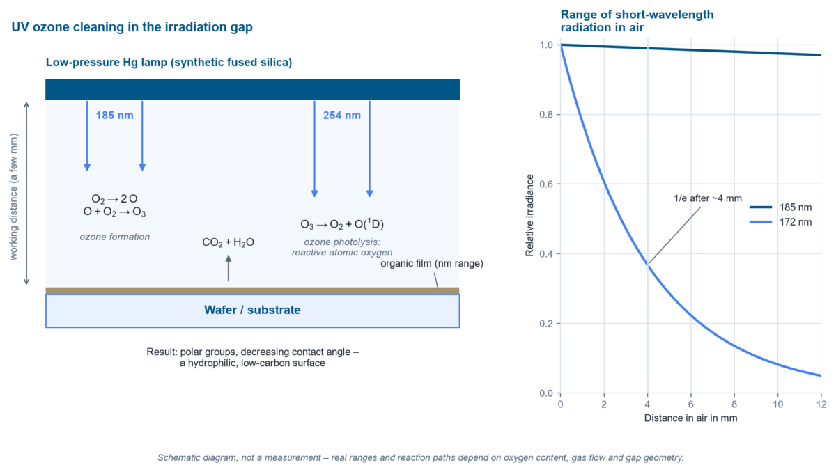
The classical process with a low-pressure mercury lamp made of synthetic fused silica uses two resonance lines. The 185 nm line dissociates molecular oxygen; the resulting oxygen atoms form ozone with O₂. The 254 nm line is strongly absorbed by ozone in the Hartley band and splits it again, producing mainly excited atomic oxygen O(¹D). This highly reactive intermediate oxidises hydrocarbons to CO₂ and H₂O, which are removed as gas. At the same time, polar groups form at the surface, rendering silicon and oxide surfaces hydrophilic. How this process works in detail and where its limits lie is described in surface cleaning and activation with UVC and ozone.
In the VUV process with xenon excimer radiation at 172 nm, direct photolysis dominates: a photon at this wavelength carries 7.2 eV or 696 kJ/mol, which is above the bond energies of C–C, C–H and C–O bonds. In addition, oxygen is dissociated in the immediate vicinity of the surface, so that atomic oxygen is created where it is meant to act. The measurable effect of both processes is a change in surface state, not material removal: water contact angle and surface energy change, while the topography ideally remains untouched.
Which technologies are used?
| Technology | Characteristics | Advantages | Limitations | Typical application |
|---|---|---|---|---|
| Low-pressure Hg lamp, 185/254 nm | line spectrum; about 40 % of the electrical power at 254 nm, around 6–9 % at 185 nm; synthetic fused silica required | large-volume ozone generation, robust, large working distances possible | mercury, warm-up behaviour, temperature and ageing drift of the line ratios, ozone extraction required | cleaning and activation of wafers, substrates, housings and joining surfaces |
| Xe₂ excimer, 172 nm (VUV) | quasi-monochromatic, 7.2 eV photon energy; radiant efficiency around 10 % | direct bond scission, very low thermal load, effective at short times | range in air limited to a few millimetres; gap geometry and gas flow are process-critical | activation before direct and hybrid bonding, cleaning of glass, polymers and wafer surfaces |
| KrCl excimer, 222 nm | quasi-monochromatic, 5.6 eV; considerably less ozone generation than 172/185 nm | operation in air with less ozone management | lower photon energy, more selective in its effect | cleaning of temperature- and ozone-sensitive assemblies |
| UV LED, 365/385/405 nm | narrowband, typical FWHM 10–15 nm; wall-plug efficiency at 365 nm today in the 40–55 % range | fast switching, stable dose control, no mercury, long lifetime | no ozone generation, unsuitable for oxidative cleaning; emission maximum shifts with junction temperature | exposure of g-/h-/i-line photoresists, curing, wafer edge exposure |
| UV-C LED, 255–280 nm | narrowband; wall-plug efficiency currently in the single- to barely double-digit percentage range | mercury-free, compact, can be deployed with pinpoint accuracy | power density and efficiency limited; generates no ozone | disinfection, selected photochemical tasks, sensing |
| Hg medium-/high-pressure lamp, g-/h-/i-line | lines at 365, 405, 436 nm plus continuum | high power over a large area, established resist processes | ageing changes the line ratios, high thermal load, regulatory time limit | mask aligner and proximity exposure, thick-film resists |
| Excimer laser, 248/193 nm | pulsed, coherent, high peak intensity | highest resolution in projection lithography | equipment and cost, highly specialised resist chemistry | front-end patterning |
| EUV, 13.5 nm | photon energy 92 eV; vacuum and reflective optics required | smallest feature sizes | outside the UV range in the narrower sense; stochastic effects at low doses | advanced logic and memory nodes |
UV exposure of photoresist: g-, h- and i-line
Photoresists are not threshold materials with a fixed cut-off wavelength; they have absorption bands. Classical positive resists based on diazonaphthoquinone and novolak are exposed in the range of the i-line (365 nm) and the h- and g-lines (405 nm, 436 nm). Exposure converts the photoactive compound; the exposed areas become soluble in the developer. Chemically amplified resists (CAR) for DUV and EUV work differently: exposure generates an acid that only acts catalytically during the post-exposure bake. The result then no longer depends on the optical dose alone but additionally on the thermal budget.
Typical dose ranges for orientation: thin i-line positive resists in a mask aligner need about 65 to 110 mJ/cm², thick-film resists for redistribution layers of 8 to 20 µm in an i-line stepper on the order of 180 mJ/cm², EUV resists about 30 to 90 mJ/cm² depending on the resolution target. These values are always valid only in connection with the spectral composition of the source for which they were determined.
Which process quantities are decisive?
| Process quantity | Unit | Why it governs the process |
|---|---|---|
| Spectral irradiance at the point of process | mW/(cm²·nm) | Only the fraction that falls within the absorption band of the resist or adsorbate acts chemically. Two sources with the same broadband reading can have completely different effective fractions. |
| Radiant exposure (dose) | mJ/cm² | For simple first-order photoreactions it determines the degree of conversion. It is the integral of irradiance over time, not the process time itself. |
| Irradiance distribution across the area | % deviation | Non-uniformity translates directly into critical-dimension scatter and locally incomplete cleaning. |
| Oxygen partial pressure and gas flow | vol %, l/min | At 172 nm and 185 nm the reactive species is first created in the gas phase. Too little oxygen limits the oxidation; sluggish gas flow leaves reaction products in the gap. |
| Working distance in the irradiation gap | mm | At VUV wavelengths the radiation is absorbed by oxygen itself. The distance thus controls both the radiation supply and the radical formation. |
| Substrate and resist temperature | °C | Affects adsorption, diffusion of the photoacid, development kinetics and – with LEDs – the emission wavelength of the source. |
| Layer thickness and absorption coefficient of the resist | µm, µm⁻¹ | Determines the dose profile over depth and thus the edge profile. With thick layers the dose at the bottom of the layer lies well below the surface dose. |
| Temporal profile of the irradiance | mW/cm²(t) | With chemically amplified systems and oxygen-inhibited reactions, the profile cannot be traded arbitrarily against time. |
What limits the process or leads to defects?
Electrical power is not optical dose. The fraction of the electrical power that arrives at the point of process as usable radiation in the relevant spectral range is in the region of a few per cent to a few tens of per cent for gas discharge lamps, and it falls over the lifetime. Reflector ageing, window clouding and deposits act multiplicatively. An unchanged power reading does not rule out a dose loss of several tens of per cent.
Time alone is not a process quantity. A specification such as “60 s irradiation” is reproducible only within an unchanged equipment configuration. As soon as lamp, distance, window or gas flow change, the dose shifts without the time indicating it.
The 185 nm fraction is often overestimated or not present at all. Low-pressure mercury lamps generate ozone only if the bulb is made of synthetic fused silica with high VUV transmission. Doped bulbs deliberately block 185 nm. Two lamps with identical 254 nm specifications can therefore show completely different cleaning behaviour.
At 172 nm the atmosphere itself limits the range. The absorption cross-section of molecular oxygen at 172 nm is about 4.6 · 10⁻¹⁹ cm². In air at standard conditions this gives an attenuation to 1/e after roughly 4 mm and by 90 % after about 10 mm. A working distance of 20 mm therefore does not mean “somewhat less dose” but practically no VUV radiation at the surface at all. At 185 nm the cross-section is about two orders of magnitude lower; there, distances of several centimetres are sensible.
Photon energy is necessary but not sufficient. A 254 nm photon carries 471 kJ/mol, nominally above the bond energy of a C–C bond. Saturated hydrocarbons, however, barely absorb at this wavelength. The cleaning effect at 254 nm therefore arises mostly indirectly via ozone photolysis. Anyone using 254 nm without a sufficient ozone budget loses the dominant reaction path.
More dose is not always better. With overly long VUV treatment of silicon the surface roughness increases measurably – in studies on direct bonding from 0.30 nm RMS in the initial state to about 0.94 nm after 25 min at 10 mW/cm². The contact angle has long since saturated by then. The process thus has an optimum, not a monotonic behaviour.
Recontamination is faster than expected. Activated surfaces are thermodynamically unstable. Hydrocarbons from ambient air, packaging and neighbouring materials re-adsorb within minutes to hours. The time between activation and joining is therefore one of the process parameters.
Contact angle and dose measure different things. The dose proves that a defined radiation input took place. The contact angle or surface energy proves that the desired surface state was reached. Neither quantity replaces the other.
Measuring next to the point of process is not the point of process. With gap dimensions of a few millimetres, with irradiance fall-off at the edges and with shadowing topography, the value at the component surface differs considerably from the value at the sensor position in the chamber wall.
How do spectrum, material and geometry influence the process?
The spectral influence acts on three levels. First, on the source side: a data sheet value of “365 nm” describes the centroid of a distribution. FWHM, secondary maxima and – with LEDs – the temperature-dependent shift of the emission maximum of typically a few tenths of a nanometre per kelvin change the effective fraction. With gas discharge lamps the ratios between the g-, h- and i-lines shift over the lifetime.
Second, on the material side: photoresists and photoinitiators have absorption bands with steep flanks. A shift of the source by a few nanometres can change the absorbed fraction by several per cent up to tens of per cent. With thick-film resists, depth dependence is added: following Lambert-Beer, the irradiance decreases exponentially, so surface and bottom dose diverge. Strongly absorbing systems produce sloped sidewalls as a result, reflective substrates additionally produce standing waves.
Third, on the geometry side: in VUV cleaning the irradiation gap is a reaction space, not a transport path. The mean free path of atomic oxygen at atmospheric pressure is in the range of a few micrometres, so the reactive species is consumed close to where it is created. Increasing the distance not only reduces the irradiance but also moves the radical formation away from the surface. With structured components, shadowing, edge over-irradiation and – in deep trenches and blind holes – limited gas exchange come on top. The ozone concentration itself also acts geometrically: at 1000 ppm ozone, about 13 % of the 254 nm radiation is absorbed over a 5 mm path, at 5000 ppm about half. High ozone concentration therefore does not increase the effect indefinitely but begins to shield the radiation that drives it.
How can the process be described quantitatively?
Three relations suffice to calculate the essential interdependencies.
Photon energy. From E = h · c / λ follows the molar photon energy. It decides which bonds can be split directly at all.
| Wavelength | Photon energy | Molar energy | Reference bond energies |
|---|---|---|---|
| 172 nm | 7.21 eV | 696 kJ/mol | C–H ≈ 413 kJ/mol |
| 185 nm | 6.70 eV | 647 kJ/mol | C–C ≈ 346 kJ/mol |
| 222 nm | 5.58 eV | 539 kJ/mol | C–O ≈ 358 kJ/mol |
| 254 nm | 4.88 eV | 471 kJ/mol | Si–O ≈ 452 kJ/mol |
| 365 nm | 3.40 eV | 328 kJ/mol | O=O ≈ 498 kJ/mol |
Lambert-Beer law. E(z) = E₀ · exp(−α · z) describes both the attenuation of VUV radiation in the oxygen-containing gap and the dose profile in the resist layer. The absorption coefficient α depends on wavelength and concentration; for gases α = σ · n with the absorption cross-section σ and the particle density n. The model assumes homogeneous absorbers, absence of scattering and constant optical properties. In photoresists the last assumption is violated as soon as bleaching sets in.
Exposure kinetics after Dill. For a positive resist, to first order M/M₀ = exp(−C · E), where M is the concentration of the photoactive compound, E the dose and C the Dill parameter with the unit cm²/mJ. As long as this description holds, the product of irradiance and time is the governing quantity – the reciprocity law is satisfied. The practical consequence: halving the irradiance at twice the time gives the same result. This statement loses its validity when a second, non-photon-driven reaction is involved – such as acid diffusion in the post-exposure bake of chemically amplified resists, oxygen inhibition in thick layers or thermal effects at high irradiance. Irradiance and time then become independent parameters.
Worked example: photon demand for removing a hydrocarbon film
Assumptions. Adventitious hydrocarbon film of 2 nm thickness, density 1 g/cm³, mean building unit CH₂ at 14 g/mol. Irradiation at 172 nm. Photon energy 1.155 · 10⁻¹⁸ J.
Model. Area-related number of building units N = d · ρ · NA / M; required photon number NPh = N / Φ with the effective quantum yield Φ for the complete removal of one building unit; dose H = NPh · EPh.
Calculation. N ≈ 8.6 · 10¹⁵ cm⁻². At an ideal yield of Φ = 1 the dose would be about 10 mJ/cm². Realistically, several photons are needed per building unit to be removed, because recombination, gas-phase absorption and incomplete oxidation cause losses. For Φ = 0.1 this gives about 100 mJ/cm², for Φ = 0.03 about 330 mJ/cm².
Result and interpretation. At a typical VUV irradiance of 10 mW/cm² at the surface, 100 mJ/cm² corresponds to about 10 s. Observed process times of several minutes until a contact angle below 5° is reached lie well above that. The difference is not a contradiction but the actual information: it quantifies the losses due to gas-phase absorption, removal of reaction products and diffusion limitation. Anyone wanting to transfer process times must therefore know the irradiance at the point of process; the time specification alone is not transferable.
Worked example: dose error caused by spectral mismatch
Assumptions. i-line positive resist with a dose-to-clear of 110 mJ/cm², contrast γ = 3. Exposure with a medium-pressure lamp, monitored with a broadband radiometer calibrated at 365 nm whose responsivity, however, also captures components at 405 nm and 436 nm.
Model. The reading corresponds to the integral over srel(λ) · Eλ dλ. If the lamp's line ratio shifts over its lifetime, the reading changes differently from the effective dose. The remaining resist thickness approximately follows Δd/d ≈ −γ · ΔE/E.
Calculation. A spectral mismatch of 10 % means, at γ = 3, a relative change of the developed layer thickness of around 30 %.
Interpretation. The contrast of the resist amplifies dose errors. The one-time spectral characterisation of the source is therefore not a formality but the prerequisite for any subsequent broadband monitoring to remain interpretable at all.
Where are UV cleaning and UV exposure used?
Semiconductor front end. Cleaning and activation before deposition, oxidation or bonding; photostabilisation; wafer edge exposure after resist coating. Critical here are freedom from particle contamination and the reproducibility of the interface state across the entire wafer, right into the edge region.
Advanced packaging and assembly. Exposure of thick resists for redistribution layers, temporary bonding and UV debonding, potting and encapsulation, cleaning before wire bonding, soldering and molding. The critical process quantity is the dose across the entire, increasingly large-format area and the dose at the bottom of thick resist layers.
Direct and hybrid bonding. VUV/O₃ activation creates hydrophilic, low-carbon surfaces and enables bond strengths at considerably lower temperatures than conventional hydrophilic bonding. Critical are contact angle, roughness increase and the time until joining.
Sensor and optics manufacturing. UV activation before bonding glass, quartz, ceramics and plastics; exposure of structured functional layers. Critical are the spectral match between source and initiator and the avoidance of material damage at short wavelengths.
Automotive electronics and power electronics. Cleaning before joining power modules, potting and encapsulation with high demands on adhesion under thermal cycling. Critical is a documented dose history, because the process result can hardly be tested non-destructively on the finished module.
Medical technology and life science devices. Activation of polymers and microfluidic substrates, exposure of resists for microstructures. Critical are material compatibility and documented process parameters.
Research and metrology. Irradiation chambers with defined, homogeneous irradiance for kinetics studies, material ageing and the determination of action spectra.
What helps with blind holes, temperature-sensitive assemblies and ozone avoidance?
- Low-oxygen processes. If direct photolysis without oxidative ozone chemistry is to dominate at 172 nm, the gap is inerted with nitrogen. The range of the VUV radiation then increases considerably and the oxidative component largely disappears – the process shifts from oxidation to bond scission and rearrangement.
- Temperature-sensitive assemblies. Excimer sources at 172 nm and 222 nm as well as LED systems operate with low infrared load; the thermal stress on the substrate stays low, which is decisive for already mounted components and polymers.
- Selective irradiation of small areas. For wafer edges, bond pads and joining surfaces, masked systems or systems designed as line or spot sources are sensible; the homogeneity check must then be performed in the same geometry as the process.
- Deep structures and blind holes. Where gas exchange is limiting, neither more irradiance nor more time alone helps. Effective are pulsed operation with purge phases, pressure cycling or a switch to processes with different transport characteristics.
- Ozone avoidance. Where ozone is undesirable for occupational safety or material reasons, 222 nm sources, doped lamp bulbs or low-ozone process atmospheres are options; the cleaning effect demonstrably shifts, so the process must be requalified.
Which quantities must be measured or monitored?
The measurement task follows directly from the process task. For UV cleaning and activation the target quantity is the surface state; water contact angle or surface energy are measured by established methods, supplemented by methods for determining residual carbon. These quantities are not process control variables, however, because they are determined by sampling and outside the process. The controllable reference variable is the radiant exposure at the point of process, supplemented by the ozone concentration or the oxygen content in the gap.
For the UV exposure of photoresist the target quantity is the absorbed dose in the resist layer. What is measured is the irradiance in the wafer plane, integrated over the exposure time, plus the homogeneity across the exposure area.
When choosing the measurement method:
- A spectral measurement is required when a source is characterised for the first time, when technologies are compared – say, mercury lamp versus UV LED –, when a resist or initiator change is due or when ageing effects on the line spectrum are suspected. Only the spectral irradiance makes it possible to calculate the effective fraction within the absorption band – measured with a spectroradiometer such as the UVpad or the SR900.
- A broadband measurement is sufficient for the routine monitoring of a qualified, spectrally known process – for recurring handheld measurements, say, with the RMD Pro. The prerequisite is that the spectral responsivity of the sensor matches the source spectrum and that the spectral mismatch has been quantified.
- Spatially resolved measurements become necessary when large areas, edge regions or several sources are involved.
- Time-resolved measurements become necessary with pulsed operation, with conveyor systems and with chemically amplified systems in which reciprocity is not assured.
The requirement is not the interface but the validity of the transmitted value. A structure of three levels makes sense.
Level 1 – reference characterisation. Spectral measurement of the source in process geometry, once and after every intervention. The results are the relative spectrum, the homogeneity map and the conversion factors between the point of process and the permanently installed sensor position.
Level 2 – stationary process monitoring. Permanently installed, temperature-stabilised sensors at a defined position continuously deliver irradiance and, derived from it, the dose per component – inline sensors remain permanently in the beam path, the PLC.net delivers its values to the controller via Ethernet, the PLC.D covers serial connection and triggered operation. Critical is transferability: without the factor determined in level 1, the sensor describes only itself.
Level 3 – control and traceability. From the measured dose, lamp or LED power is adjusted, ageing trends are detected and maintenance intervals are derived. The dose per component is archived together with identification, timestamp and equipment state. This makes a process documentable whose result can no longer be tested non-destructively on the end product.
Technically significant is the transition from time control to dose control: a system that controls to a target dose compensates lamp ageing and window clouding on its own, as long as the sensor is calibrated and the conversion factor is valid. A system that runs on time loses this compensation entirely. How such measurement chains are integrated into control environments is described on the market page UV technology for automation and process integration.
The main contributors to measurement uncertainty are spectral mismatch, deviation from the ideal cosine response, temperature and linearity effects of the detector, and the positioning uncertainty in the irradiation gap. With VUV measurements there is the added factor that the sensor itself is part of the absorption path: sensor geometry and gas flow around it change the reading. A traceable calibration – for instance by an ISO/IEC 17025 accredited calibration laboratory – fixes the systematic part of this uncertainty, but does not replace the application-specific assessment of the spectral mismatch.
What do scientific publications show?
Five works provide the technical basis for the central statements of this text on cleaning mechanism, process optimum and exposure kinetics:
- Fundamentals of UV/ozone cleaning. The systematic consolidation of the mechanisms – direct photolysis, ozone formation at 185 nm, ozone photolysis at 254 nm and the importance of small distances between lamp and surface – was achieved in a review article that serves as the reference for process design and pre-cleaning requirements to this day. – Vig, J. R.: UV/ozone cleaning of surfaces, Journal of Vacuum Science & Technology A 3(3), 1027–1034, 1985.
- VUV/O₃ activation for low-temperature direct bonding. The study examined the effect of 172 nm irradiation at 10 mW/cm² and 2 mm distance on silicon and fused silica. The water contact angle drops from around 70° to below 2° within a few minutes, the bond strength at 200 °C exceeds values of conventional hydrophilic processes at 400 °C, while the roughness increases considerably with overly long irradiation. The work demonstrates both the effectiveness and the existence of a process optimum. – Xu, J.; Wang, C.; Wang, T.; Wang, Y.; Kang, Q.; Liu, Y.; Tian, Y.: Mechanisms for low-temperature direct bonding of Si/Si and quartz/quartz via VUV/O₃ activation, RSC Advances 8, 11528–11535, 2018.
- Dose-dependent material change through UV ozone. On two-dimensional semiconductors it was shown that UV ozone treatment tunes optical and electrical properties deliberately, but degrades them irreversibly beyond an optimal treatment duration. For process practice it follows that “cleaned” and “unchanged” do not hold simultaneously for arbitrarily long. – Sarcan, F., et al.: Ultraviolet-Ozone Treatment: An Effective Method for Fine-Tuning Optical and Electrical Properties of Suspended and Substrate-Supported MoS₂, Nanomaterials 13(23), 3034, 2023.
- Quantitative description of photoresist exposure. The introduction of the quantities later known as the Dill parameters A, B and C created the basis for treating exposure as a kinetic process with measurable material constants instead of running it empirically on time specifications. – Dill, F. H.; Hornberger, W. P.; Hauge, P. S.; Shaw, J. M.: Characterization of positive photoresist, IEEE Transactions on Electron Devices 22(7), 445–452, 1975.
- Absorption and photon statistics of modern resists. Measurements of dynamic absorption coefficients show that at short wavelengths and low doses the number of absorbed photons per volume becomes so small that statistical effects co-determine the process window. This explains why dose reduction cannot be realised arbitrarily as a productivity gain. – Fallica, R.; Stowers, J. K.; Grenville, A.; Frommhold, A.; Robinson, A. P. G.; Ekinci, Y.: Dynamic absorption coefficients of chemically amplified resists and nonchemically amplified resists at extreme ultraviolet, Journal of Micro/Nanolithography, MEMS, and MOEMS 15(3), 033506, 2016.
UV exposure and microstructuring in customer publications
UV exposure and microstructuring also appear in several facets in the publications of Opsytec customers – from photolithography in microfluidic chips to the dose-dependent material response of a photoresist.
Shows that hydrogel microstructures in microfluidic chips can be produced with simple UV photolithography at VLSI-capable density – exposure dose and mask geometry determine the achievable structural fidelity.
Hydrogel patterns in microfluidic devices by do-it-yourself UV-photolithography suitable for very large-scale integration
Beck, Anthony, et al. "Hydrogel patterns in microfluidic devices by do-it-yourself UV-photolithography suitable for very large-scale integration." Micromachines 11.5 (2020): 479.
Measures the exposure-dependent refractive index of a photoresist – direct evidence that the absorbed dose determines the material properties beyond mere pattern transfer.
Exposure-dependent refractive index of Nanoscribe IP-Dip photoresist layers
Dottermusch, Stephan, et al. "Exposure-dependent refractive index of Nanoscribe IP-Dip photoresist layers." Optics letters 44.1 (2018): 29-32.
Uses photolithographically microstructured polymer carriers for serial crystallography at synchrotrons – UV microstructuring outside classical chip manufacturing, with the same demands on dose and homogeneity.
Micro-structured polymer fixed targets for serial crystallography at synchrotrons and XFELs
Carrillo, Melissa, et al. "Micro-structured polymer fixed targets for serial crystallography at synchrotrons and XFELs." IUCrJ 10.6 (2023).
Examines UV-induced degradation of silicon heterojunction solar cells under defined irradiation – the same question of dose and spectrum, asked of the finished semiconductor device.
Passivating Contacts-Related Ultraviolet-Induced Degradation in Silicon Heterojunction Solar Cells
Xu, Binbin, et al. "Passivating Contacts-Related Ultraviolet-Induced Degradation in Silicon Heterojunction Solar Cells." Small Structures 7.6 (2026).
Further works from related fields are compiled in the publications by customers, sorted by topic.
Technical fundamentals and further sources
- Vig, J. R.: UV/ozone cleaning of surfaces. Journal of Vacuum Science & Technology A 3(3), 1027–1034 (1985). DOI 10.1116/1.573115 – mechanisms of UV/ozone cleaning, distance dependence, pre-cleaning requirements.
- Dill, F. H.; Hornberger, W. P.; Hauge, P. S.; Shaw, J. M.: Characterization of positive photoresist. IEEE Transactions on Electron Devices 22(7), 445–452 (1975). DOI 10.1109/T-ED.1975.18159 – kinetic description of exposure, Dill parameters A, B, C.
- Xu, J., et al.: Mechanisms for low-temperature direct bonding of Si/Si and quartz/quartz via VUV/O₃ activation. RSC Advances 8, 11528–11535 (2018). DOI 10.1039/C7RA13095C – 172 nm activation, contact angle, bond strength, roughness limit.
- CIE 220:2016, Characterization and Calibration Method of UV Radiometers, together with CIE S 017/E:2020 (ILV; the earlier German classification to DIN 5031-7:1984 has been withdrawn without a successor) – definition of the UV spectral ranges, spectral mismatch, calibration and characterisation methods for UV radiometers.
- ISO 19403-2, Wettability – Determination of the surface free energy of solid surfaces by measuring the contact angle, and DIN EN ISO/IEC 17025:2018-03, General requirements for the competence of testing and calibration laboratories – normative foundations for surface assessment and traceable radiation measurement.
- SEMI, Mid-Year Total Semiconductor Equipment Forecast (2026), WSTS Semiconductor Market Forecast, Spring 2026 and Yole Group, Status of the Advanced Packaging Industry (2025) – market indicators for front-end, back-end and advanced-packaging investment; each cited with its year.
FAQ on UV cleaning and UV exposure in semiconductor manufacturing
How does UV ozone cleaning of wafers work?
Short-wavelength UV radiation splits bonds in organic adsorbates and simultaneously generates ozone and atomic oxygen from the oxygen in the air. These reactive species oxidise hydrocarbons to CO₂ and H₂O. The process is dry, non-contact and low-particle; the result shows up as a falling water contact angle and rising surface energy.
Which wavelength is suitable for UV cleaning of semiconductor surfaces?
The 185/254 nm combination from low-pressure mercury lamps acts mostly indirectly via ozone formation and ozone photolysis and allows larger working distances. Xenon excimer radiation at 172 nm additionally acts directly, because its photon energy of 7.2 eV is above the bond energies of C–C, C–H and C–O. 222 nm is an option when ozone is to be avoided.
Why does 172 nm cleaning fail at a larger distance?
Molecular oxygen absorbs strongly at 172 nm. In air at standard conditions the irradiance falls to 1/e after about 4 mm and to a tenth after roughly 10 mm. At the same time, the reactive oxygen is then no longer created at the surface. Usual working distances are therefore in the range of 1 to 3 mm.
Which dose is required for the UV exposure of photoresist?
The dose depends on resist type, layer thickness, substrate reflection and source spectrum. Thin i-line positive resists typically need 65 to 110 mJ/cm² in a mask aligner, thick-film resists for redistribution layers on the order of 180 mJ/cm². Such values are transferable only together with the spectrum for which they were determined.
What is the difference between irradiance and radiant exposure?
Irradiance in mW/cm² describes the radiant power per area arriving at this moment. The dose in mJ/cm² is its integral over time. For first-order photoreactions the dose determines the conversion. As soon as diffusion or thermal processes are involved, the irradiance becomes an independent parameter. How irradiance, dose and fluence differ formally is set out in the overview of radiometric quantities.
Why is the electrical lamp power not sufficient to assess the process?
Only part of the electrical power is converted into usable radiation of the relevant spectral range, and only part of that reaches the component surface. Reflector ageing, window clouding, distance and absorption in the process atmosphere act multiplicatively. An unchanged electrical power does not rule out a considerable dose loss. Why a power rating is not a measurand in principle is derived under radiometric quantities.
How is the UV dose measured in production equipment?
First the source is characterised spectrally in process geometry and the relation between the point of process and the permanent sensor position is determined. A calibrated broadband sensor at a fixed position then takes over the routine monitoring. The dose is archived per component to be able to demonstrate ageing trends and process deviations.
When is a spectral measurement strictly required?
At the first characterisation of a source, when comparing different technologies such as mercury lamp and UV LED, when changing resist or photoinitiator, and when ageing shifts of the spectrum are suspected. Broadband measurements can conceal systematic errors of several tens of per cent in these cases.
Related application fields
Photochemical surface treatment links semiconductor manufacturing to neighbouring fields: optics and precision components uses the same UV-ozone and VUV activation on optical surfaces, photovoltaics runs comparable wafer processes including UV-induced degradation, and UV bonding, potting and encapsulation describes the joining steps that follow activation.
Author: Dr. Mark Paravia
Dr.-Ing. Mark Paravia is the managing director of Opsytec Dr. Gröbel GmbH in Ettlingen and heads the accredited calibration laboratory. Following his research on pulsed xenon excimer discharges at the Institute of Lighting Technology at KIT, his current focus is on optical radiation measurement technology. He is a recognized UV expert, vice-chair of the DIN Standards Committee FNL 7 “Optical Radiation,” and a member of the DVGW Project Group on UV Disinfection.
Consulting on UV process measurement
Unclear how much irradiance at 172 nm actually arrives at the wafer surface in a gap a few millimetres wide – or how much dose remains at the bottom of a 15 µm resist layer? A spectral measurement in process geometry and a traceable calibration of the sensors in use clarify whether a process window is real or merely nominal – write to us with your question.