

UV Technology for Optics and Precision Components – Cleaning, Activation, Bonding and Testing
For optical precision components, the surface is the function. Manufacturers use ultraviolet radiation in optics production at three distinct points: to photochemically remove organic films, to activate glass and polymer surfaces before coating or bonding, and to cure transparent adhesives when joining lenses, prisms, filters and light guides. In all three cases the technical goal is the same: a reproducible, documented radiant dose at the point of action. The central difficulty is that the workpiece is itself an optical element with a defined, often deliberately limited transmission - it changes the very radiation that is meant to cure or clean it. The decisive quantities are the spectral irradiance at the component, the dose integrated from it, the photon energy of the wavelength used, and the local oxygen concentration.
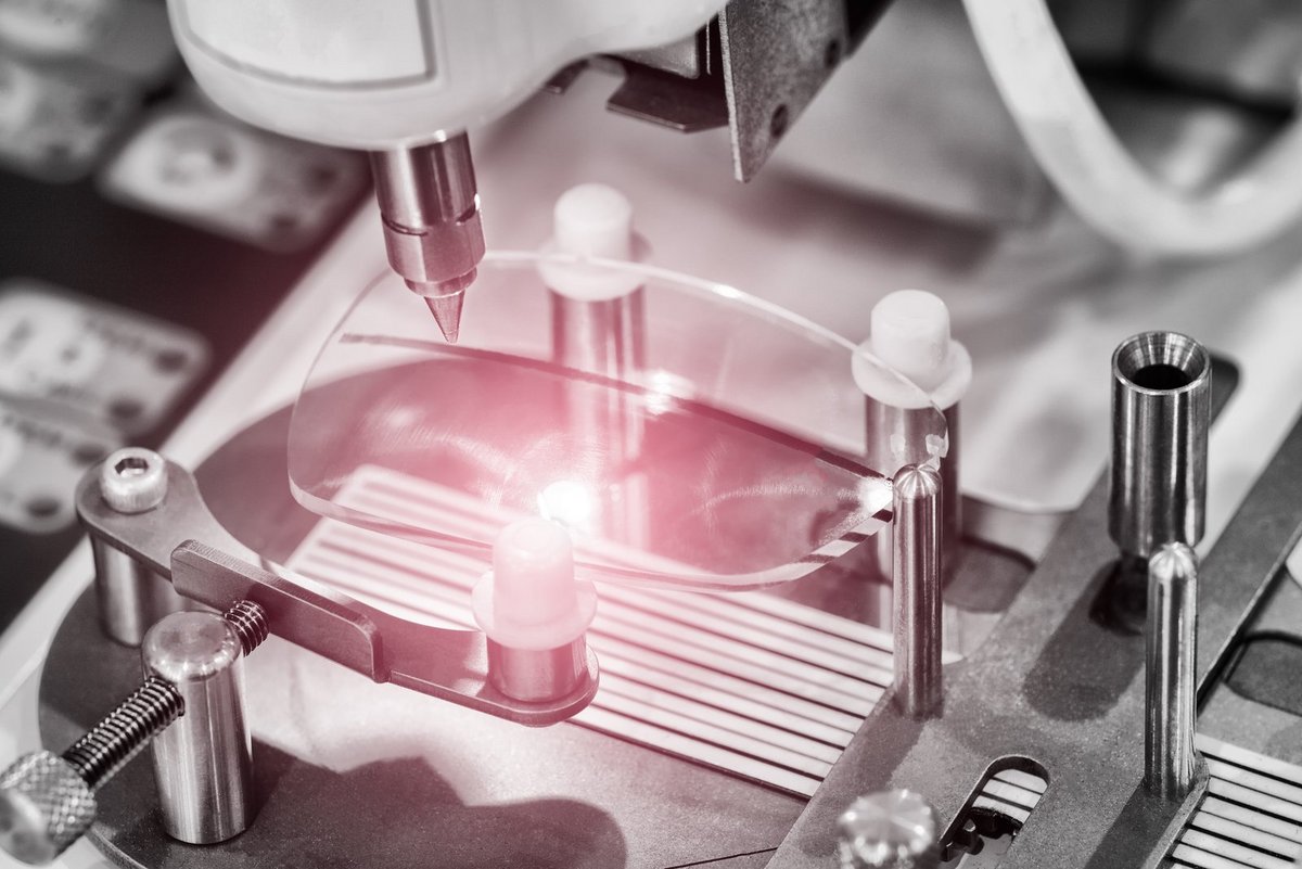
How is the market for optical precision components developing?
In 2024, the German photonics industry generated roughly €50 billion in revenue at an export ratio of 76.3 percent and employed around 188,000 people across some 1,000 companies (SPECTARIS, Key Data 2025). Within this industry, the "components and materials" segment is the largest single segment at 27 percent of production value - optical components are therefore not a niche of photonics but its quantitative core. Globally, the components-and-materials sub-segment reached US$122.9 billion with average annual growth of 7.4 percent between 2019 and 2022 (Photonics21/TEMATYS, Market Research Study Photonics 2024); passive optical components including coatings accounted for US$38 billion of that, of which more than 80 percent falls in the visible range and around 4 percent in UV components.
The value-chain structure explains the tolerance requirements: systems and subsystems made up about 86 percent of the photonics market in 2022, components 14 percent. A single component therefore carries a small share of the value but decides the function of an assembly worth six to seven figures - a faulty bond on a €40 lens can render an entire objective or lithography module unusable. This asymmetry is the economic reason why process monitoring is such a cost-effective lever in optics manufacturing.
Four sub-markets are currently driving requirements in particular:
- Semiconductor lithography. SEMI forecast fab equipment spending of US$124 billion for 2026. This is where the tightest cleanliness budgets in all of optics manufacturing apply.
- Automotive LiDAR and camera modules. The automotive LiDAR market grew to US$859 million in 2024 and is projected to reach US$3.56 billion by 2030 (Yole Group, 2025). High unit volumes shift the problem from the individual assembly to overall process capability.
- AR optics. Among AR glasses, the share of waveguide-based devices rose within a single year from 13 percent (H2 2024) to 38 percent (H2 2025) (Counterpoint Research, 2026). Diffractive waveguides are manufactured on a wafer basis, which requires uniform area exposure rather than point irradiation.
- Laser optics. The world market for laser sources stood at US$19.3 billion in 2022, of which US$1.4 billion was excimer lasers. UV laser optics are especially sensitive to residual contamination because it lowers the laser damage threshold.
The technical chain behind these figures is consistent throughout: rising unit volumes and smaller components push manufacturing toward wafer-based, automated process chains; these rule out mechanical and wet-chemical cleaning; they shift bonding toward fast-curing UV adhesives; and in return they demand measurable, logged radiometric quantities in place of experience values.
Five developments are shifting the boundary conditions of optics manufacturing:
- Regulatory shift toward mercury-free sources. For mercury-containing UV lamps, the time-limited RoHS exemptions expire on 24 February 2027; whether an extension would follow had not been decided as of 2026 (details under RoHS and UV Lamps – Current Regulations and Developments). Anyone switching from medium- or low-pressure sources to UV LED changes the spectrum at the same time - process windows, adhesive approvals and sensor calibrations all need to be re-established. For research, instrument calibration and reference standards, mercury-containing sources are exempted under the Minamata Convention, so they are likely to remain available in metrology longer than in production.
- New wavelengths. Available power at 265 nm and 222 nm broadens the process toolkit toward mercury-free UVC. The consequence for metrology: sensors and calibrations must cover these wavelengths, and a chain calibrated at 254 nm does not transfer.
- Wafer-based optics manufacturing. Precision glass moulding at wafer level, nanoimprint for diffractive structures, and metasurfaces are shifting optics manufacturing into semiconductor process chains. The technical consequence: processes must be uniform over area and dry, and the governing quantity shifts from point irradiance to the distribution across the wafer.
- Additive optics manufacturing. When inkjet-printing optical elements from hybrid polymers, UV curing occurs between print layers. Dose per layer determines dimensional accuracy, interlayer adhesion and residual monomer content, and therefore directly determines optical quality - layer-by-layer dose control becomes part of the manufacturing file.
- Standards updates. Several standards central to optics have recently been revised: ISO 9211-1 to -3 in February 2024, ISO 10110-6 and -11 in 2025, ISO 13696 on total scatter in 2022, and ISO 11551 on absorption of optical laser components is undergoing revision. An overview of these and other standards is available under Guidelines, Standards and Norms in UV. Specifications should always state the part number and edition year.
How does the photochemical treatment of optical surfaces work?
Photochemical cleaning and activation exploit the fact that short-wavelength UV photons carry more energy than typical bonds in organic molecules. Photon energy is about 7.2 eV at 172 nm, 6.7 eV at 185 nm and 4.9 eV at 254 nm. For comparison, C-C bonds sit around 3.6 eV and C-H bonds around 4.3 eV. Radiation below 200 nm therefore breaks organic bonds directly.
A parallel oxidative pathway runs alongside it. Oxygen does not dissociate until wavelengths below about 242 nm; the 185 nm line of a low-pressure mercury lamp generates atomic oxygen from O₂ and, from that, ozone. The same lamp's 254 nm line splits ozone again at the peak of its Hartley band, releasing excited atomic oxygen. This strongly oxidising intermediate mineralises the hydrocarbon fragments broken open earlier into CO₂ and H₂O, which are carried away as gases. The process runs contact-free, without solvents and without introducing particles - which is why it is attractive for coated surfaces that cannot tolerate mechanical cleaning. Process, limitations and typical components are described under Surface Cleaning and Surface Activation with UVC and Ozone; for a closed-chamber setup, the BS-OX is the corresponding instrument.
At 172 nm (Xe₂ excimer), the direct photolytic pathway dominates because oxygen absorption at this wavelength is so high that the radiation penetrates only a few millimetres of air. Working distance thus becomes a process parameter in its own right. The trade-off is unavoidable: whatever oxidises organic compounds also attacks the organic constituents of a component. Plastic optics, cement layers, ink markings and some soft coatings therefore need individual compatibility testing before process release - compatibility is a materials question, not a process question.
Which technologies are used?
| Technology | Characteristics | Advantages | Limitations | Typical application |
|---|---|---|---|---|
| Low-pressure mercury lamp, 185/254 nm | Two lines, low power density, quartz bulb without phosphor | Ozone generation and ozone photolysis from a single source; very low residual contamination achievable | Long process times; ozone extraction required; contains mercury | Precision cleaning of lenses, prisms, filters and substrates before coating and bonding |
| Amalgam lamp, 254 nm | Higher power density, temperature window for optimum operation | Shorter cycle times in area processes | 185 nm fraction low depending on bulb material; temperature-dependent output | Cleaning of large-area substrates and wafer carriers |
| Xe₂ excimer lamp, 172 nm | Narrowband VUV emission from a dielectric barrier discharge, mercury-free | High photon energy, activation within seconds, site-selective via masks | Range in air only a few millimetres; inerting or minimal working distance required; specialised VUV metrology | Activation of polymer optics, cyclic olefin components and glass before joining |
| KrCl excimer lamp, 222 nm | Narrowband, mercury-free | Greater range than 172 nm, less material damage | Little ozone generation; weaker cleaning effect on thick films | Gentle activation of sensitive coatings |
| Medium-pressure mercury lamp | Broadband from UVC to VIS, high radiant power, IR fraction | High cure depth for thick adhesive layers | Heat load shifts alignment; broad spectrum also strikes blocking filters | Curing large-volume bonds and potting compounds |
| UV LED, 265 to 405 nm | Narrowband, instantly switchable, dimmable, mercury-free | Wavelength tunable to photoinitiator and component transmission; low heat load on the component; high local irradiance | Ages with operating hours and junction temperature; no UVC below 250 nm at relevant power | Spot curing when bonding lenses, fibres and sensor windows |
| Excimer and solid-state lasers, 193/248/266/355 nm | Coherent, high peak pulse power | Structuring, material removal, damage-threshold testing | Not an area process; risk of laser-induced damage | Micro-structuring, qualification of DUV optics |
| Oxygen or argon plasma | Physico-chemical attack via ion bombardment | Very fast activation, also on inorganic residues | Ion bombardment can damage interference coatings and soft coatings; vacuum required | Alternative where photochemical processes are not sufficient |
The spectral distribution of common UV source types - including both mercury-lamp lines and the excimer lamps - is documented in the spectral database for UV lamps, a useful starting point for technology selection.
Which process quantities are decisive?
Spectral irradiance at the point of action (mW/cm²·nm). It determines how many photons of which energy actually reach the component per unit time. Only the spectrally resolved quantity allows comparison with the absorption of the photoinitiator and the transmission curve of the component. The underlying radiometric quantities - irradiance and dose - are defined under Radiometric Quantities: Irradiance and Dose.
Radiant exposure, i.e. dose (mJ/cm²). The time integral of irradiance governs conversion when bonding and residual contamination when cleaning. Dose is the acceptance-relevant quantity because it can be documented as a single value - but it does not replace stating the irradiance at which it was reached.
Photon flux density. From irradiance and photon energy follows the number of photons per area and time. At 365 nm, 1 mW/cm² corresponds to roughly 1.8 · 10¹⁵ photons per cm² and second, at 265 nm only about 1.3 · 10¹⁵. The same irradiance therefore means fewer, but more energetic, photons at the shorter wavelength.
Oxygen partial pressure and atmosphere. In photochemical cleaning, oxygen is a reaction partner; in radical photopolymerisation it is an inhibitor. The same quantity acts with opposite sign in the two processes.
Working distance and geometry. At 172 nm, oxygen absorption limits the useful range to a few millimetres, at 185 nm it extends to the centimetre range. In addition, irradiance from point sources falls off roughly with the square of distance.
Temperature. It affects the output of amalgam and medium-pressure lamps, the efficiency and wavelength of UV LEDs, reaction kinetics via the Arrhenius relation, and, through thermal expansion, the alignment of the assembly.
Layer thickness and joint geometry. In absorbing adhesives, irradiance falls off exponentially with depth. Joint depth and adhesive absorption therefore decide whether a bond cures through or only cross-links at the surface.
Uniformity and angle of incidence. In area and wafer processes, non-uniformity of irradiance sets the process window, because the weakest region of the field sets the minimum dose and the strongest sets the material load.
What limits the process, and what causes failures?
Electrical lamp power is not an optical dose. The relationship between connected electrical power and usable irradiance at the component depends on source efficiency, reflector condition, bulb clouding, distance and ageing. In mercury-based sources in particular, the short-wavelength fraction drops much faster than total output - a source can still appear nominally "bright" while having already lost most of its 185 nm fraction.
Time instead of dose, in the wrong order. Time-controlled processes implicitly assume that irradiance stays constant. It does not: lamps age, LED junction temperatures drift, windows become contaminated and solarise. A fixed exposure time is only valid if irradiance is measured regularly and the time is adjusted accordingly.
Limits of the reciprocity law. The assumption that half the irradiance and double the time give the same result holds for photopolymers only within a limited range. The termination kinetics of radical polymerisation depend nonlinearly on irradiance, and the validity of the Bunsen-Roscoe law varies with resin viscosity. Process windows must therefore be verified experimentally for each formulation.
Oxygen inhibition at open joints. At exposed adhesive surfaces, oxygen competes with the monomer for radicals. The result is tacky surfaces, incomplete conversion and outgassing during later operation - even with a correctly measured dose. Countermeasures are higher irradiance, inerting, or an adjusted formulation.
Over-treatment during activation. Photochemical activation raises surface energy, but at excessive dose it also oxidises the substrate: plastic optics yellow or become brittle at the surface, metal and fluoride coatings oxidise, cement layers and ink markings are attacked. The process has an upper dose limit - more is not automatically better.
Hydrophobic recovery. The wettability produced by activation is time-limited. Polymer chains reorient, and the surface becomes less polar again over hours to days. The window between activation and joining is a process parameter that is frequently left unspecified.
The component as a filter. A UV-blocking filter does not transmit curing radiation by design; a bandpass filter only within a narrow window. Quartz glass is transparent well below 200 nm, borosilicate glass such as N-BK7 becomes practically opaque below about 320 nm, and plastic optics made of PMMA or cyclic olefin have their own cut-off. A dose figure measured in front of the component does not describe the dose in the joint.
Measuring at the wrong location. A measurement at the lamp output or outside the chamber captures neither absorption by components and windows nor reflection and shadowing effects within the assembly. At 172 nm, the air path between the sensor head and the reference plane additionally dominates the result.
Spectral mismatch of broadband sensors. A filter-based radiometer weights the spectrum with its own spectral responsivity. If the source changes - say, from a medium-pressure lamp to a 385 nm LED - the reading changes even though the physical irradiance stays the same. Comparisons between source types require a spectral measurement or a documented mismatch correction.
Position drift after joining. Adhesives shrink as they cross-link. In actively aligned assemblies at sub-micrometre precision, this shrinkage shifts the component position during and after cure; post-cure and moisture uptake produce a delayed post-cure shift. Residual stress in the component is not a side issue either: multi-point bonds create stress birefringence and surface-form errors that show up as wavefront error.
Which material, spectral and geometry effects are commonly underestimated?
Transmission edges of the substrate. The usable wavelength is set by the substrate, not the adhesive: synthetic fused silica is usable down to about 185 nm, calcium fluoride down to around 130 nm, classic crown glasses only into the long UV-A. When irradiating through the component, this edge decides whether any photons reach the adhesive at all.
Solarisation and point defects. UV exposure generates point defects in fused silica such as E' centres, non-bridging oxygen hole centres and oxygen-deficiency centres. Their formation and annealing depend on OH content, chlorine and fluorine content, and hydrogen loading. In practice: entrance optics, light guides and diffusers in UV instruments drift over their service life - a physical reason for defined recalibration intervals, not merely a formal QM requirement.
Angular shift of interference filters. The pass wavelength of an interference filter shifts to shorter wavelengths at oblique incidence. With an effective index of 1.7, an angle of incidence of 20 degrees produces a shift of roughly 2 percent, turning 365 nm into about 358 nm. A curve recorded at normal incidence therefore no longer correctly describes use in a converging beam path. The same effect limits the accuracy of filter-based radiometers.
Regular versus total transmission. At scattering, matte or structured surfaces, regular and total transmittance are two different numbers. Which one is correct follows from the application: imaging quality depends on the regular fraction, the energy balance of a curing process on total transmission. Without stating the measurement geometry, a transmission value is not interpretable.
Stray light grows disproportionately in the UV. At equal roughness, surface scattering scales approximately with λ⁻⁴. A polish that is unremarkable in the visible can violate stray-light limits in the DUV. Roughness and stray-light figures are also only comparable if the spatial frequency or angular band captured is stated alongside them.
Molecular contamination. At short wavelengths, atomic layer thicknesses already matter: model calculations for EUV lithography show that a reflectance loss of one percent per mirror corresponds to roughly five atomic layers of carbon, and with around ten mirrors in a tool this adds up to roughly ten percent throughput loss; permissible hydrocarbon partial pressures lie around 10⁻¹² mbar (ASML Research, 2016). Low-outgassing adhesives - typically screened to ASTM E595 with mass loss below 1 percent and condensable content below 0.1 percent - and low-contamination, oxidation-gentle cleaning processes are therefore a prerequisite, not an add-on.
Expert section: dose, Beer-Lambert, and the limits of the models
Radiant exposure - dose, in industry usage - is the time integral of irradiance: H = ∫ Ee(t) dt, or H = Ee · t for constant irradiance. Here H is radiant exposure in mJ/cm², Ee is irradiance in mW/cm², and t is exposure time in seconds. The simple product form assumes a temporally constant source; for pulsed or gated systems and for moving components, integration is mandatory.
Inside an absorbing medium - adhesive, tinted glass, photoresist - irradiance falls off according to the Beer-Lambert law: Ee(z) = Ee(0) · e^(–αz), with α = ε · c. Here z is depth, α the absorption coefficient, ε the molar extinction coefficient of the photoinitiator, and c its concentration. This gives the most important practical consequence: dose is not a property of the component but a function of position. The material parameters behind this relationship - critical energy density and penetration depth - can be determined radiometrically and describe at what dose, and at what depth, gelation sets in.
Limits of the model. Beer-Lambert assumes a fixed, unconsumed absorber concentration. During photopolymerisation, however, the initiator is consumed, the medium bleaches as exposure proceeds, and absorption shifts over time. Scattering in the adhesive, reflections at bonded interfaces and oxygen diffusion from the surroundings are also not captured. The law therefore gives a lower-bound estimate of cure depth and an explanation for depth gradients - not an exact process prediction.
Worked example: what exposure time is needed behind a UV-attenuating component?
Assumptions. A sensor window with a transmittance of 12 percent at 365 nm is bonded onto a mount. The adhesive specification requires a dose of 3,000 mJ/cm² at 365 nm in the joint. The UV LED spot delivers 200 mW/cm² at 365 nm at the top of the component. The adhesive layer is a thin 100 µm, and its own absorption is neglected for a first approximation.
Model. Ejoint = τ · Etop, and t = H / Ejoint.
Calculation. Ejoint = 0.12 · 200 mW/cm² = 24 mW/cm²; t = 3000 / 24 = 125 s.
Result. Instead of the 15 seconds derived from the irradiance at the top surface, 125 seconds are actually required - a factor of 8.3.
Technical interpretation. This calculation is a lower bound. At only 24 mW/cm², polymerisation proceeds more slowly, which lets oxygen from the surroundings diffuse further into the joint during the extended exposure; the reciprocity assumption - that the same dose at lower irradiance gives the same conversion - is not guaranteed in this regime. The dose actually required may therefore be higher still. Three practical ways out exist: choose a wavelength at which the component shows higher transmission; irradiate from the joint side with a UV LED spot; or switch to an adhesive with a better-matched initiator absorption. In all three cases the irradiance in the plane of the joint must be verified by measurement, not derived by calculation.

Where is UV technology used in optics manufacturing?
Semiconductor and lithography optics. UV is used for the dry final cleaning of substrates, masks and mount parts, because even a monomolecular hydrocarbon film can lead to carbon deposition under short-wavelength exposure. The critical process variable is residual contamination after treatment, controlled indirectly via applied dose and ozone concentration - the same variable that plays a central role in electronics and semiconductor manufacturing.
Automotive sensing. Camera modules and LiDAR assemblies are bonded with UV adhesives in high volumes because fixing and alignment can be combined in a single cycle-time step. What matters is reproducibility of irradiance across every nest of a machine, since otherwise process capability - not just the individual joint - fails; the integration of such metrology into cycled machines is covered in depth on the Automation and Process Integration market page.
AR and micro-optics. Wafer-level optics, embossed waveguides and metasurfaces require area-wide activation and curing with defined uniformity. The critical variable is non-uniformity of irradiance across the wafer.
Medical technology and endoscopy. Distal optics, fibre bundles and windows are bonded with biocompatible, sterilisable adhesives. What matters is complete conversion, because unreacted residual monomer is extractable and jeopardises biocompatibility testing; dose documentation is part of process validation.
Laser optics. Before coating, surface cleanliness determines the laser-induced damage threshold. What matters here is that the cleaning dose is high enough for the organic residue layer and low enough for coating compatibility.
Datacom and integrated photonics. When coupling fibres to photonic chips, UV fixing follows active alignment at sub-micrometre precision. What matters is cure shrinkage, because it directly degrades coupling efficiency.
Space and vacuum optics. Here, the requirement for complete cure combines with outgassing qualification of the adhesives. What matters is degree of conversion and post-cure, because incompletely cross-linked fractions later condense on cold optical surfaces and are then photo-fixed there under UV exposure.
Research and metrology. In calibration and testing laboratories, defined UV exposure serves to characterise materials, sensors and sources. What matters is traceability of irradiance to national standards.
What helps with 172 nm processes, concealed joints and thick adhesive layers?
In VUV processes around 172 nm, oxygen absorption limits the usable path length. Technical answers are inerted chambers with nitrogen purge, minimised working distances in the millimetre range, and metrology calibrated at exactly this wavelength - a sensor calibrated at 254 nm gives no valid reading at 172 nm.
For assemblies where the joint is not directly accessible, radiation is routed either through light guides or via reflections within the component. How the field is actually distributed in an angled assembly can be estimated before building the fixture with optical simulation; the simulation does not, however, replace the final measurement in the joint, because scattering at engineering surfaces and alignment tolerances are only partly modellable.
For temperature-sensitive assemblies, narrowband UV LEDs replace broadband sources because the IR fraction, and with it thermally induced misalignment, is eliminated - ready-built, for instance, as a UV LED spot with LEDControl Touch as a controllable driver. For very thick or strongly absorbing adhesive layers, a broadband source can conversely be necessary, because longer wavelengths there carry the depth effect.
Where ozone is undesirable in the process but activation is still required, low-ozone wavelengths such as 222 nm or near-surface VUV processes come into play; where ozone is the actual active agent, the chamber must control ozone concentration and residence time reproducibly.
Which quantities need to be measured or monitored?
The measurement task follows from the application, not the other way round. The first question is which physical quantity governs the process: for photochemical cleaning it is the radiant exposure in the short-wave UVC combined with ozone concentration; for bonding it is the irradiance in the photoinitiator's absorption range and the resulting dose; for activation it is the dose in the range that breaks the relevant bonds. The measurement location follows next: the component surface for cleaning, the joint for bonding. Measurements taken outside that plane are auxiliary quantities and are only valid once the correlation has been documented.
Broadband measurement with a filter-based radiometer is sufficient as long as the source and spectrum remain unchanged and only changes over time are being tracked. It is robust, fast, and suited to routine production monitoring.
Spectral measurement with a spectroradiometer such as the SR900 or the UVpad is required whenever source types are compared, wavelengths are changed, adhesives are qualified, or component transmission curves need to be taken into account. For processes around 172 nm, dedicated VUV metrology such as the tinyTracker 172 nm is needed, because off-the-shelf sensors are not calibrated there.
Dose measurement at flat or narrow joints is handled by flat data loggers such as the curelog or by irradiation chambers with defined geometry such as the UV-MAT; for reproducible material qualification in the lab, irradiation chambers are available more generally.
Total transmission of scattering or structured components is captured by integrating spheres or the Cary 60 integrating sphere, because they also collect the scattered fraction. For transmission at a fixed process wavelength in incoming-goods and batch inspection, process photometers are the appropriate choice.
In automated production lines, measurement moves from spot-checking into the process itself. Inline sensors in the irradiation plane continuously supply irradiance, from which the machine controller integrates dose per workpiece - connected digitally via PLC.D or PLC.net. The technical significance lies not in the interface but in the control variable: when dose, not time, is regulated, the machine automatically compensates for source ageing, window contamination and the temperature dependence of UV LEDs. Without this feedback, the process result drifts along with the lamp's service life.
Digital sensors with a direct link to the controller allow limit monitoring with an early-warning threshold: a first threshold triggers maintenance before a second threshold blocks parts. Combined with per-workpiece data logging, this produces the traceability chain that regulated industries require anyway and that, in the event of a fault, allows affected batches to be identified precisely.
For statistical evaluation, keep in mind that an inline sensor represents one position, not the whole field. Demonstrating the capability of a UV measuring system therefore requires a correlation between the sensor position and the component plane, plus a regular reference measurement with a traceable instrument. Only then is ongoing monitoring metrologically linked to process release.
Measurement uncertainty budgets should include at least calibration uncertainty, spectral mismatch, cosine error at non-normal incidence, linearity across the measurement range, the sensor's temperature dependence and its long-term stability. The authoritative reference for the design, characterisation and calibration of UV radiometers is CIE Publication 220:2016. Only traceability to national standards makes dose figures comparable between supplier and customer at all - which is what the calibration laboratory accredited to ISO/IEC 17025 provides.
What do scientific publications show?
- Foundations of UV/ozone cleaning. Vig described in 1985, systematically, the interplay of 185 nm ozone generation, 254 nm ozone photolysis and atomic oxygen, and established that it is the irradiance actually reaching the component - not lamp power - that determines cleaning effectiveness. - Vig, J. R.: UV/ozone cleaning of surfaces, Journal of Vacuum Science & Technology A 3(3), 1027–1034, 1985.
- Choosing wavelength and discharge type for excimer sources. Kogelschatz, Esrom, Zhang and Boyd summarised in 2000 the fundamentals of incoherent UV and VUV excimer radiation for low-temperature materials processing. - Kogelschatz, U. et al.: High-intensity sources of incoherent UV and VUV excimer radiation for low-temperature materials processing, Applied Surface Science 168, 29–36, 2000.
- VUV activation, quantified. Hozumi and co-workers showed how the water contact angle of polymer surfaces decreases with 172 nm dose, and that working distance and residual oxygen in the gap dominate the effective dose. - Hozumi, A.; Inagaki, H.; Kameyama, T.: The hydrophilization of polystyrene substrates by 172-nm vacuum ultraviolet light, Journal of Colloid and Interface Science 278(2), 383–392, 2004.
- Limits of the reciprocity law. Wydra and co-workers tested the reciprocity law on dimethacrylate systems in 2014, both theoretically and experimentally, and showed that it holds only within a limited range. - Wydra, J. W. et al.: The reciprocity law concerning light dose relationships applied to BisGMA/TEGDMA photopolymers, Dental Materials 30(6), 605–612, 2014.
- Oxygen inhibition. Ligon and co-workers reviewed the state of the art on oxygen inhibition in photopolymerisation in 2014, explaining the typical residual tackiness of open joints and the effectiveness of inerting and raised irradiance. - Ligon, S. C. et al.: Strategies to Reduce Oxygen Inhibition in Photoinduced Polymerization, Chemical Reviews 114(1), 557–589, 2014.
- Molecular contamination of optical surfaces. Hollenshead and Klebanoff modelled in 2006 the radiation-induced carbon growth on EUV optics as a function of hydrocarbon partial pressure and photon flux; these results still underpin permissible residual concentrations in manufacturing and measurement environments today. - Hollenshead, J. T.; Klebanoff, L. E.: Modeling radiation-induced carbon contamination of extreme ultraviolet optics, Journal of Vacuum Science & Technology B 24(1), 64–82, 2006.
- Stray-light parameters compared across methods. Duparré and co-workers showed in 2002 that roughness and stray-light figures for optical surfaces are only comparable when the spatial-frequency band captured is stated - a limitation that acceptance specifications frequently omit. - Duparré, A. et al.: Surface characterization techniques for determining the root-mean-square roughness and power spectral densities of optical components, Applied Optics 41(1), 154–171, 2002.
What do customer publications show?
Refractive index of UV-cured photoresist for two-photon lithography of micro-optical structures - the same question as when bonding through an optical component: how does UV exposure change the optical properties of the cured material itself?
Exposure-dependent refractive index of Nanoscribe IP-Dip photoresist layers
Dottermusch, Stephan, et al. "Exposure-dependent refractive index of Nanoscribe IP-Dip photoresist layers." Optics Letters 44.1 (2018): 29–32.
Micro-structured polymer sample holders for serial crystallography at synchrotrons and free-electron lasers - UV-structured precision components subject to the same demands on dimensional fidelity and cleanliness as an X-ray optics beamline.
Micro-structured polymer fixed targets for serial crystallography at synchrotrons and XFELs
Carrillo, Melissa, et al. "Micro-structured polymer fixed targets for serial crystallography at synchrotrons and XFELs." IUCrJ 10.6 (2023).
Outgassing monitoring of a silicone adhesive for spacecraft assemblies under vacuum-UV exposure - the outgassing problem named above as critical for space and vacuum optics, measured directly on the adhesive itself.
Multiparameter Single Sensor for Space Silicone Adhesive Monitoring Under High-Vacuum Ultraviolet Exposure
Fazzi, Luigi, et al. "Multiparameter Single Sensor for Space Silicone Adhesive Monitoring Under High-Vacuum Ultraviolet Exposure." Journal of Spacecraft and Rockets 60.3 (2023): 740–752.
Technical foundations and further sources
Normative reference documents: ISO 10110 (drawing indications for optical elements, parts 6 and 11 in the 2025 edition), ISO 9211-1 to -3:2024 (optical coatings), ISO 13696:2022 (total scattering), ISO 11551 (absorption of optical laser components), ISO 14644-1:2015 and ISO 14644-8:2022 (cleanroom, chemical air cleanliness), ASTM E595 (outgassing), DIN 5031-10:2018 (photobiologically effective radiation), DIN EN ISO/IEC 17025:2018-03 (competence of testing and calibration laboratories), and CIE 220:2016 (characterisation and calibration of UV radiometers) - an overview of the relevant standards and guidelines is also available under Guidelines, Standards and Norms in UV.
Market figures: SPECTARIS Key Data 2025 and Trend Report Photonics 2025/2026; Photonics21/TEMATYS Market Research Study Photonics 2024 (2022 data basis); SEMI World Fab Forecast (June 2025); Yole Group and Counterpoint Research (commercial market studies, 2025/2026).
FAQ on UV processes for optics and precision components
How is an optical surface cleaned with UV radiation?
Short-wavelength UV radiation breaks organic bonds directly, while the 185 nm line generates ozone from atmospheric oxygen and the 254 nm line splits that ozone back into atomic oxygen. The atomic oxygen oxidises the molecular fragments to CO₂ and water, which are carried away as gases. The process is contact-free and solvent-free, but removes only organic films - not particles and not salts.
Which wavelength is suitable for bonding optical components?
Two curves matter: the absorption of the photoinitiator and the transmission of the component being irradiated through. Quartz glass transmits well below 200 nm, borosilicate glass practically only above about 320 nm, and UV-blocking filters block by design. In practice, 365 nm, 385 nm and 405 nm are used; for strongly attenuating components, irradiation is instead carried out from the joint side.
What dose is required?
The dose is specified by the adhesive or process supplier, typically in mJ/cm² at a defined wavelength. It is only meaningful together with the irradiance and the measurement location, because the same dose value at very different irradiances does not necessarily give the same conversion. What matters is the dose in the joint, not at the top of the component.
What is the difference between irradiance and dose?
Irradiance is a power density in mW/cm² and describes the instantaneous state. Dose, physically the radiant exposure, is its time integral in mJ/cm² and describes the total energy delivered per unit area. Two processes with the same dose can give different results if their irradiance differs. Symbols, units and the distinction from fluence are given under radiometric quantities.
The UV process is not working even though lamp power seems adequate - why?
The most common causes are ageing of the source with a disproportionate loss of short wavelengths, absorption by the component or a chamber window, an excessive working distance, oxygen inhibition at open joints, and measurement outside the plane of action. Electrical input power is not an optical dose; without a measurement at the point of action, the cause cannot be pinned down. The general derivation – from electrical power through electro-optical efficiency to the measurand at the point of action – is given under radiometric quantities.
How is the UV dose measured in a joint?
Practical options are flat measuring heads or data loggers positioned in the plane of the joint, or measurements on a representative fixture dummy with identical geometry. Where a direct measurement is geometrically impossible, a measurement is taken at an accessible position and the relationship to the joint plane is quantified and documented once.
Is a broadband radiometer enough, or is a spectrally resolving measurement needed?
A broadband radiometer is sufficient as long as the same source is being tracked over time. As soon as source types are compared, wavelengths are changed, or component transmission is taken into account, a spectral measurement is required, because filter-based sensors weight the spectrum with their own responsivity and deviate systematically as a result.
Why does the effect of an interference filter shift with the angle of incidence?
An interference filter works via the optical path length within its layers. At oblique incidence, this path shortens effectively, and the pass wavelength shifts to shorter values - by roughly 2 percent at 20 degrees. A curve measured at normal incidence therefore does not correctly describe use in a converging beam path.
Related application fields
Optical components touch on several neighbouring fields: electronics and semiconductor manufacturing shares cleaning, VUV activation and wafer-level process chains, in aerospace the same surfaces are additionally tested for radiation ageing, and transmission testing for laser processes measures the transmittance that is taken as given here.
Author: Dr. Mark Paravia
Dr.-Ing. Mark Paravia is the managing director of Opsytec Dr. Gröbel GmbH in Ettlingen and heads the accredited calibration laboratory. Following his research on pulsed xenon excimer discharges at the Institute of Lighting Technology at KIT, his current focus is on optical radiation measurement technology. He is a recognized UV expert, vice-chair of the DIN Standards Committee FNL 7 “Optical Radiation,” and a member of the DVGW Project Group on UV Disinfection.
Key technical question
Not sure what dose the adhesive actually receives in the real joint when the optical component itself attenuates the curing radiation? We determine the spectral irradiance and dose at the real point of action, evaluate the transmission and measurement geometry of your component, and derive a robust process window from it - traceable through our accredited calibration laboratory. Send us your question.